Does Applied Materials' Sculpta Threaten ASML Dominance?

Summary
- Applied Materials, Inc., a semiconductor equipment manufacturer, released Centura Sculpta last week.
- Centura Sculpta should help foundries "bypass" EUV multi-patterning, thereby reducing litho intensity in the industry.
- At first, this might seem like terrible news for ASML Holding N.V., but is this really the case?
- This idea was discussed in more depth with members of my private investing community, Best Anchor Stocks. Learn More »
SweetBunFactory/iStock via Getty Images
Introduction
Applied Materials, Inc. (NASDAQ:AMAT), a semiconductor equipment manufacturer (“semi cap”), announced Centura Sculpta last week. According to the company, this tool will help semiconductor manufacturers (“foundries” or “fabs”) reduce the need for double patterning EUV. If you don’t know what this is, don’t worry; hopefully, you'll have an idea by the end of this article.
Last week, we saw many investors claim that the announcement meant that the ASML Holding N.V. (NASDAQ:ASML) moat is not as strong as initially thought because this tool would challenge its EUV dominance. We’ll use this article to explain why this is a misguided opinion and also to help you understand why tools such as Centura Sculpta could even benefit ASML over the long term.
Without further ado, let’s start with the basics.
What is double patterning?
Double patterning involves exposing a wafer twice with EUV light to achieve the desired tip-to-tip space. There are two “lengths” you need to understand regarding semiconductors. One is the pitch, and the other one is the tip-to-tip, both illustrated in the image below:
Applied Materials Centura Sculpta Presentation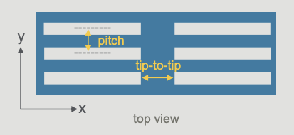
In the pattern above, pitch is basically the distance in an imaginary y-axis between interconnect lines, and tip-to-tip is the distance between interconnect lines on an imaginary x-axis.
So, where does the need for double patterning stem from? Lithography developments have focused on shrinking the pitch but have struggled to keep up with customer requirements for tip-to-tip shrink, causing what is known as the “litho gap:”
Applied Materials Centura Sculpta Presentation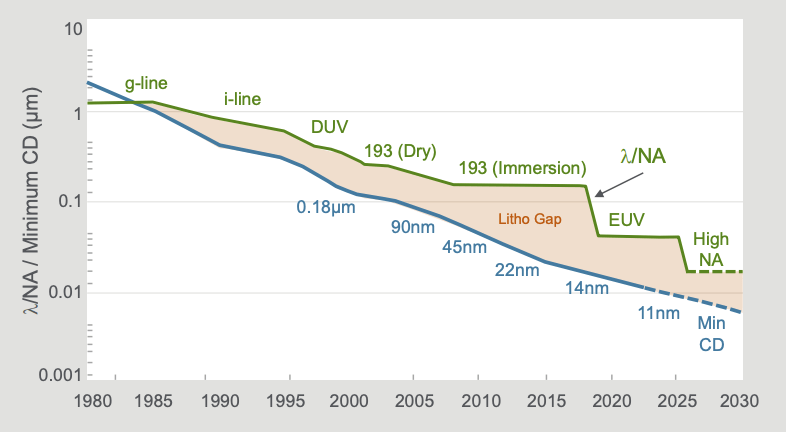
Due to the absence of alternatives, customers have been forced to expose the wafer twice with EUV light to reduce the tip-to-tip and close this gap. Applied Materials shared this graph of how double patterning works. In this case the pattern is one of "vias":
Applied Materials Centura Sculpta Presentation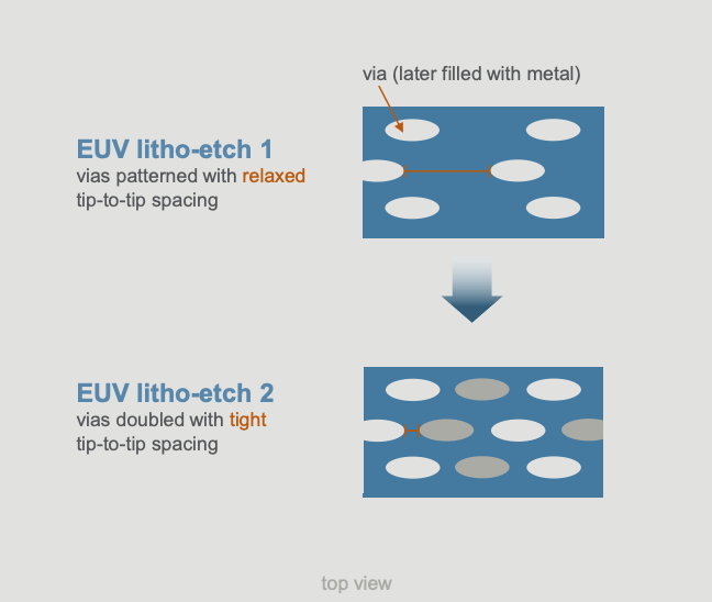
Here’s another visual that might help you understand how it works:
Applied Materials Centura Sculpta Presentation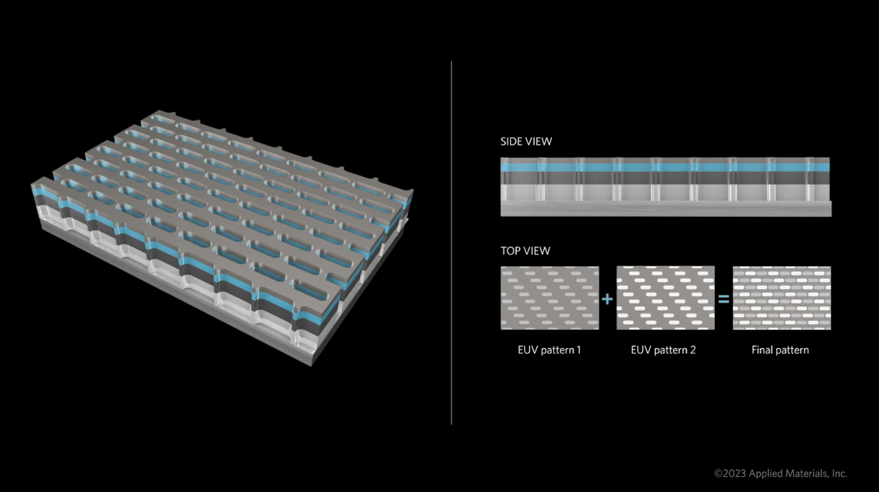
As you can see, in the first EUV exposure, the tip-to-tip remains “large,” so the manufacturer conducts a second EUV exposure with the wafer in a different position (i.e., different alignment) to print the same pattern in the empty space, thereby reducing the tip-to-tip length.
Chip manufacturers currently use multi-patterning for the most critical layers, introducing significant complexity and cost to the process. This increased complexity and cost stems from multi-patterning requiring complete chip cycles. So, for example, in the case of double patterning, the chip manufacturer would have to complete the first exposure, etch and clean the wafer and inspect it with metrology. Once this process is finished, then it has to be repeated. It’s basically like exposing two independent wafers, but in the case of double patterning, you are doing it on the same “pre-exposed” wafer:
Applied Materials Centura Sculpta Presentation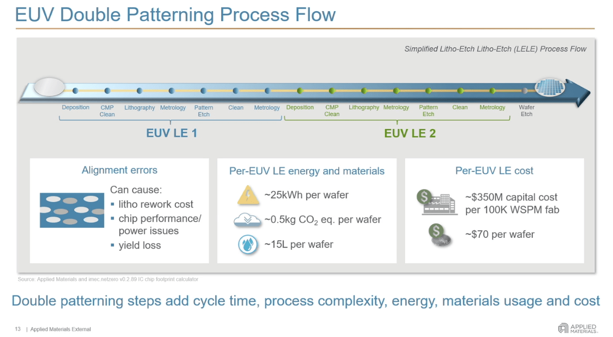
So, if the process is so inefficient both in cost and complexity, why do manufacturers do it this way? The short answer is that there’s currently no alternative. If manufacturers want to reduce the tip-to-tip to the desired level in the most advanced chip layers, their only way out is to expose the layer twice to EUV light. Applied Materials wants to reduce this need with Centura Sculpta.
What does Applied Materials’ Centura Sculpta do
Applied Materials’ new tool, Centura Sculpta, aims to eliminate the need for the second EUV exposure by “enlarging” the pre-printed pattern by exposing the wafer with a plasma at a pre-determined angle.
Centura Sculpta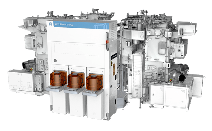
After the first EUV exposure and the subsequent metrology steps, the wafer goes into Centura Sculpta, where the printed pattern is “enlarged” to reduce the tip-to-tip space in a process called Pattern Shaping:
Applied Materials Centura Sculpta Presentation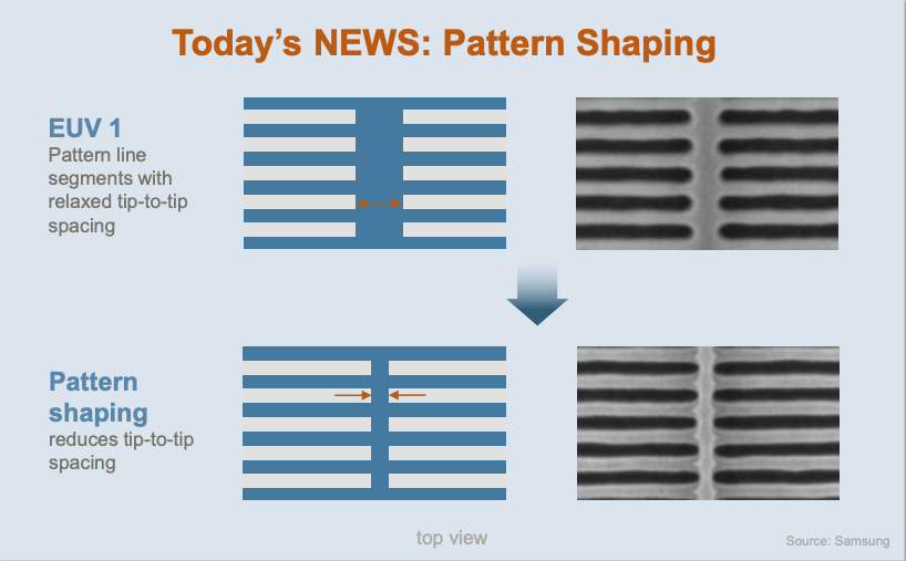
If the tool ends up being proven in high volume manufacturing, it’s obviously a significant breakthrough and has several advantages both for the foundries and the industry as a whole. For starters, it will make the manufacturing process cheaper, thereby reducing the cost of semiconductors. The semiconductor industry has complied with Moore’s law on performance over the last decade but has struggled to keep up with cost reduction. This tool should make that an achievable task.
Secondly, it can also benefit semiconductor performance. Foundries will be able to do double patterning as usual and then use Centura Sculpta to achieve what would be “triple patterning” today. And lastly, but no less importantly, the manufacturing process of semiconductors will become more environmentally friendly, as each manufacturing cycle is quite resource-intensive:
Applied Materials Centura Sculpta Presentation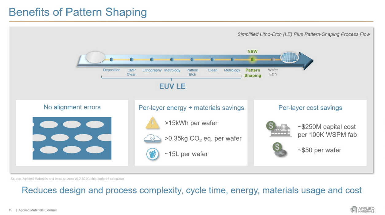
The benefits are clear, but several things remain to be answered. Let's go over some of them.
The system has been under development for 6 years. Major leading-edge foundry customers have actively participated in the development process, which is logical considering the significant productivity and cost benefits they could see. Applied Materials’ management shared quotes from some of these customers, namely Intel and Samsung. The non-appearance of TSMC in the presentation was a major surprise, considering that it’s probably the customer conducting the most EUV multi-patterning today. Of course, this could just be noise, but the fact that “only” the upstarts and not the leader are openly talking about the tool makes us believe there’s still a long way until it becomes proven in HVM.
The other question that remains to be answered concerns the types of patterns to which the tool can be applied to. During the presentation, management showed two types of patterns (interconnect lines and vias) and argued that the Centura Sculpta could be potentially applied to any pattern, although more complex patterns will take some time to adopt it. There are some doubts regarding how long it would take other patterns to adopt pattern shaping and if it will be commercially viable in cost and yield.
Of course, the last and probably most important question is how fast and where customers will adopt it. According to Applied Materials, the real value add is in EUV (even though there’s also DUV multi-patterning) and adoption will be somewhat slow. Management expects this to be a $1 billion product by 2024, which is not that high for such a “breakthrough” product. This might be caused by slow penetration until maturity is reached, which is something completely normal.
What’s important for ASML shareholders is to understand how this tool impacts the demand for the company’s EUV tools and, thus, how it impacts the long-term investment thesis, so let’s look at that.
Is it a threat to ASML’s dominance in lithography?
Many people reacted quickly to the announcement, claiming it was a clear threat to ASML. We always hesitate to respond quickly to the news because we fear we might miss something important and bias our thinking somehow. Only reading what we explained above should make it pretty clear that Centura Sculpta will not displace EUV and will be complementary. EUV will continue to be mission-critical in chip manufacturing:
Applied Materials Centura Sculpta Presentation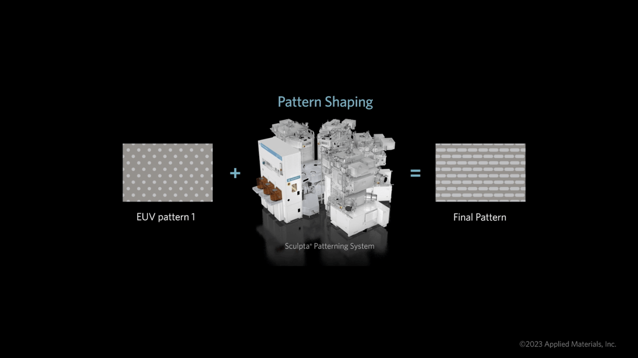
Now, it’s also evident that EUV intensity will decrease if the industry adopts Centura Sculpta. The rationale is that layers requiring multi-patterning will now require less EUV exposure, which eventually means that what two EUV systems do today might be done by one EUV system and several Centura Sculptas in the future. Of course, this is not good for ASML, but we must also look at the big picture.
High-NA will reduce the need for EUV double patterning
ASML’s customers expect to roll out high-NA EUV in HVM (high volume manufacturing) around 2025. This new system will technically reduce the need for double patterning in low-NA EUV layers, rendering Centura Sculpta less useful to reduce double patterning (emphasis added):
We are developing High-NA. High-NA is about to be launched around '24, '25. And that will be used for reducing the double-patterning EUV.
Source: Martin Van den Brink, ASML’s CTO, during Capital Markets Day
Of course, if high-NA reduces the need for double patterning in low-NA EUV layers, Centura Sculpta would “jump” to high-NA EUV to eliminate the need for double-patterning there. The bottom line is that what Centura Sculpta will solve now for low-NA EUV today is something that high-NA EUV would technically solve starting in 2025.
Of course, cost should also be a consideration here. Will high-NA EUV be more cost-efficient in reducing double patterning than a single EUV exposure and Centura Sculpta? This is honestly something that we don’t have an answer to, but there’s obviously a possibility that the value of high-NA to reduce double patterning might decrease with the adoption of Centura Sculpta. Following what Martin van Den Brink also said at Capital Markets Day (emphasis added):
So that means the value we can assign to the tool is depending how much cost attractive there is to short cut double-patterning.
Source: Martin Van den Brink, ASML’s CTO, during Capital Markets Day
Developments in EUV productivity might reduce the “cost gap”
Recall that in a recent interview, ASML’s CTO said that the next decade was all about improving EUV productivity. Improving EUV productivity basically means reducing the cost per EUV wafer, which has important implications for the cost gap that Centura Sculpta will supposedly provide.
If Centura Sculpta does not provide significant productivity improvements and its value proposition relies partly on the cost gap with EUV multi-patterning, the advantage will get shorter and shorter as years go by and ASML reduces the cost per EUV wafer.
Of course, the benefit of reducing complexity will probably remain because reducing the number of steps in a process reduces alignment errors. EUV improvements will also improve yield, but it’s unlikely that this gap will ever be closed. It’s true that if high-NA EUV reduces the need for low-NA multi-patterning, then the “complexity” gap would also be reduced. Double-patterning produces alignment errors, and while Centura Sculpta might correct these, we don’t know if other types of errors will surface. This is also a very important question that remains to be answered: what's the yield of a Centura Sculpta? We'll only know once the system is in HVM. Later in the article you'll understand why.
More advanced and cheaper semiconductors will drive more advanced applications, benefitting ASML
ASML’s management has consistently claimed that the company always provides conservative guidance because they don’t know how Moore’s Law will impact the industry. Peter Wennink, the company’s CEO, said the following during Capital Markets Day (emphasis added):
I think it's conservative for the simple reason that we don't know. We don't know. We simply cannot connect all the dots. And those dots are being created because the value of Moore's Law is there. We're creating more value than we create cost with every new node.
And then some intelligent company or a group of intelligent people is going to think of an application that we currently don't know of, that we cannot assess in terms of size and impact. It's basically the question you've been asking me for 25 years that Peter, what's the next killer application? And I said, same answer. I have no clue. And this is also what the CEO of one of our major customers told me when I said, why didn't you tell us you needed so much more mature tools.
We think the implications of the development of Moore’s Law have already become evident with the rise of AI in search engines, driven by the battle between Microsoft and Google. This is something few expected to happen this soon, but it should drive significant computing power and memory demand in the coming years. AI should also help technology advance faster, thereby creating new, unexpected semiconductor applications in the future.
The introduction of Centura Sculpta should help the industry comply with Moore’s Law by making the chip manufacturing process more affordable. Lower manufacturing costs should translate into lower consumer prices, increasing the penetration of leading-edge tech. This increased penetration should, in turn, increase the probability of the next “breakthrough” application.
More affordability eventually means more demand for chips and a lower barrier to entry to the leading-edge space. One of the main barriers to entry (besides knowhow) to the most advanced chips had been capital costs, but if these decrease, then we could see other foundries that have historically operated in the shadows of the big three (Intel, TSMC, and Samsung) go into the leading edge space. To be honest, we think the probability of this is quite low, but Intel and Samsung will probably have a more "capital-light" way of closing the gap with TSMC.
So, yes, fewer capital costs are evidently bad for ASML as the demand for its tools stems directly from the Capex of its customers. This is the straightforward impact. The not-so-straightforward impact is that lower manufacturing costs should help the industry comply with Moore’s Law going forward, thereby increasing the probability of the next breakthrough application from which ASML will benefit from. This last impact is almost impossible to quantify.
What does ASML have to say about this?
We also wanted ASML’s view, so we emailed the investor relations department. These are the takeaways from our conversation with them:
A cheaper lithography production cost should be good for ASML’s customers and, thus, for ASML over the long run.
Centura Sculpta does not replace lithography because it can’t achieve pitch shrink, only tip-to-tip shrink.
The company welcomes any development that helps the industry keep up with Moore’s Law.
ASML believes Centura Sculpta will go into HVM in around 2 years, time in which customers should validate the technology and make sure it doesn’t have any side impacts on other shapes composing the die.
The application of the technology can’t be simulated, so a lot of metrology will be necessary to test it out.
Our main doubt related to this announcement was if ASML’s management knew about it when setting its ambitious guidance on Capital Markets Day. So we asked IR, and this is what they answered (emphasis added):
At the CMD we have clearly stated that litho is not the only innovation engine. So we expected and welcome other technology innovation steps. Based on our current understanding we believe that this technology features within the boundaries of our expectations at the CMD.
We understand this as management reiterating the guidance, at least with the current available information. There are many moving parts for any business, and the fact that litho intensity might go down due to Centura Sculpta does not automatically mean that ASML will do worse as a business. Lower costs in chip manufacturing are expected to directly benefit the industry and thus benefit ASML indirectly with the rise of future advanced applications.
We will honestly like to tell you we have a way of quantifying Centura Sculpta's impact on ASML's business, but all the unknowns make us shy away from making any prediction. It's highly likely we'll not know the impact on litho intensity until the new tool gets proven in high volume manufacturing, sometime around 2024/2025. Once this happens, then we'll have to wait and see how it competes against high-NA in reducing low-NA EUV double patterning.
What did the market think of the news?
The market initially saw the news as a threat to ASML and a breakthrough for Applied Materials, making the stock of the former drop and that of the latter increase significantly:
Ycharts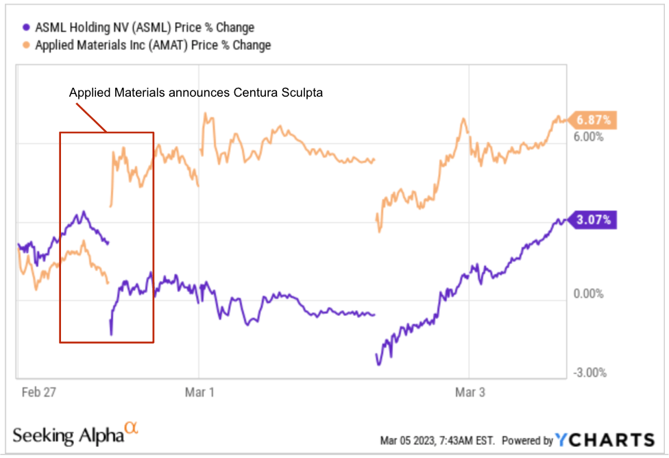
However, after the market understood the potential implications for both businesses, ASML recovered. We think that the launch of Centura Sculpta is a net positive for Applied Materials because it might allow the company to take share in a market where it wasn’t present. On the other hand, it might seem that ASML only has business to lose, but for the things we explained above, we think the net impact is uncertain at this point.
Having a monopolistic position is a double-edged sword. On the one hand, you get to enjoy all the economics of the business. On the other hand, you only have business to lose against competitors that only have business to win.
Conclusion
The news of Centura Sculpta surprised many investors, who questioned ASML's EUV monopoly. Applied Materials’ Centura Sculpta is a complementary tool to EUV, and while it’s expected to reduce litho intensity, the impact on ASML’s business is uncertain.
Centura Sculpta is still unproven in HVM. Only time will tell if the benefits it will provide customers are worth it, especially after the introduction of high-NA reduces the need for EUV double patterning and as EUV gets more productive through the decade. For us, the ASML Holding N.V. thesis remains intact with the available information. We are rating both ASML Holding N.V. and Applied Materials, Inc. as a "Hold." We don't think ASML Holding N.V. is cheap here and we have no opinion on Applied Materials, Inc.
In the meantime, keep growing!
Editor's Note: This article discusses one or more securities that do not trade on a major U.S. exchange. Please be aware of the risks associated with these stocks.
Best Anchor Stocks helps you find the best growth stocks to outperform the market with the lowest volatility. They can anchor your portfolio on the stormy market sea, still allowing you to outperform.
Best Anchor Stocks have a long track record of revenue growth combined with below-average volatility. The first pick is up 16,000% from its IPO but has never been down 30%, not even during in 2008-2009.
Best Anchor Stocks can serve several purposes: stabilize your high-growth portfolio, or add low-volatility growth to your index, dividend or value investing.
There's a 2-week free trial, so don't hesitate to join Best Anchor Stocks now!
This article was written by

But you get much more: spreadsheets, a live portfolio, chat with fast response for all your questions, webinars (we just did one to explain DCFs) and much more.
Best Anchor Stocks was founded by Kris and Leandro. Kris is known as From Growth To Value and his marketplace Potential Multibaggers and is also a finfluencer with 85k followers on Twitter.He is 45-year old and always focuses on the long term.
Leandro is the main contributor and he has a background is in Economics with a specialization in Finance. He prepared for the CFA exam for two years and, although he didn’t end up taking the exam due to two cancellations during the pandemic, it has helped him achieve a more detailed understanding of financial markets and accounting.
Both Kris and Leandro are both calm and steady in their approach and character when it comes to investing. They focus on the next years, not the next month. Price action doesn’t affect their decisions, fundamentals do. This can help investors who act based on emotions weather difficult times in the markets.
Disclosure: I/we have a beneficial long position in the shares of ASML either through stock ownership, options, or other derivatives. I wrote this article myself, and it expresses my own opinions. I am not receiving compensation for it (other than from Seeking Alpha). I have no business relationship with any company whose stock is mentioned in this article.