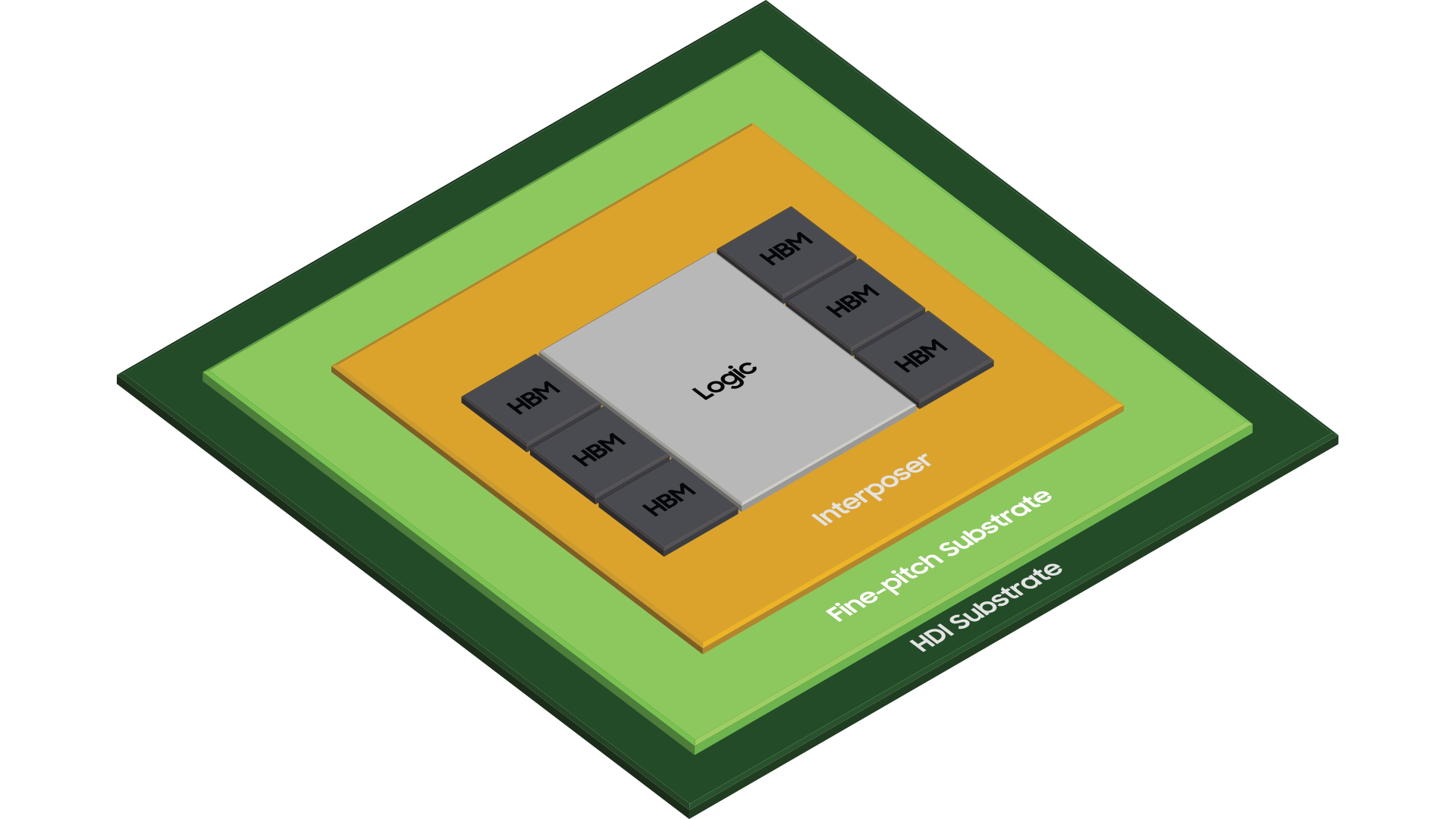
Samsung Foundry has announced that its latest 2.5D semiconductor chip packaging technology H-Cube is now available for its foundry clients. H-Cube, which was developed in collaboration with Samsung Electro-Mechanics and Amkor Techology, allows complex logic and HBM (High-Bandwidth Memory) chips to be packed in compact sizes.
The South Korean firm said that its new packaging technology is suitable for AI (Artificial Intelligence), data center, HPC (High-Performance Computing), and networking products that require high-performance and large-area packaging. This technology can be used to place logic chips or HBM on top of a silicon interposer in a smaller area.
To develop this technology, Samsung Foundry used a hybrid substrate with a fine-pitch substrate and High-Density Interconnection (HDI) to fit large sizes into 2.5D packaging. With increasing computing power and storage needs, semiconductor chips can become larger in size, but 2.5D chip packaging technology like H-Cube can fit more in a smaller area and offer compact solutions.
When fitting six or more HBMs in a single package, difficulty in making the package can increase rapidly. Samsung solved this issue by using a hybrid substrate structure that uses an easy-to-implement HDI substrate overlapped under a fine-pitch substrate. The company also used solder balls with a smaller pitch (35%) to connect the chip with the substrate.
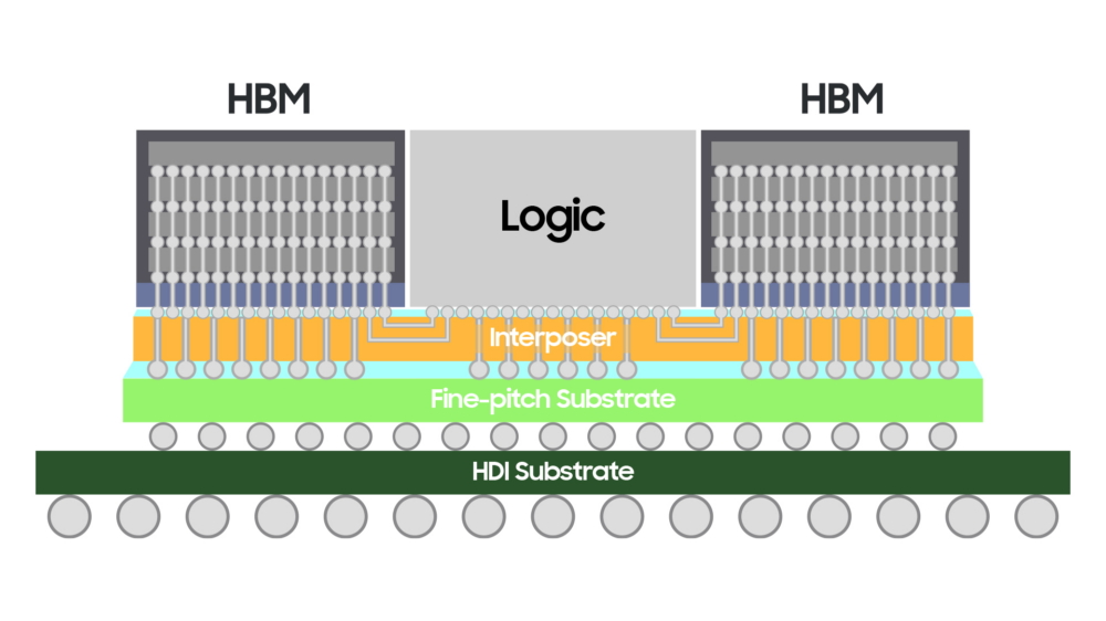
The company also used its proprietary signal/power integrity analysis technology for a stable power supply and less distortion when stacking logic chips on top of HBM.
said Moonsoo Kang, Senior Vice President and Head of Foundry Market Strategy Team at Samsung Electronics, said, “H-Cube solution, which is jointly developed with Samsung Electro-Mechanics (SEMCO) and Amkor Technology, is suited to high-performance semiconductors that need to integrate a large number of silicon dies. By expanding and enriching the foundry ecosystem, we will provide various package solutions to find a breakthrough in the challenges our customers are facing.”