“Samsung’s 5nm FinFET process technology is said to provide a 25 percent increase in logic area efficiency”
Samsung on Tuesday has announced that it has completed the development of its 5nm FinFET process technology and now is ready for customers’ samples. When compared to the 7nm, the brand’s 5nm FinFet process is said to provide up to a 25 percent increase in logic area efficiency, 20 percent lower power consumption, or 10 percent higher performance. The 5nm uses EUV lithography in metal layer patterning thus reducing mask layers while providing better fidelity.
Samsung says that the key benefit of 5nm is that it can reuse all the 7nm intellectual property on the 5nm process. This will help the company significantly reducing the migration costs, pre-verified design ecosystem, and, consequently, shorten their 5nm product development. This comes after Samsung has announced the readiness and its initial production of the 7nm process, which is its first process node with EUV lithography technology in October 2018. The company has provided commercial samples of the industry’s first EUV-based new products and has started mass production of the 7nm process early this year.
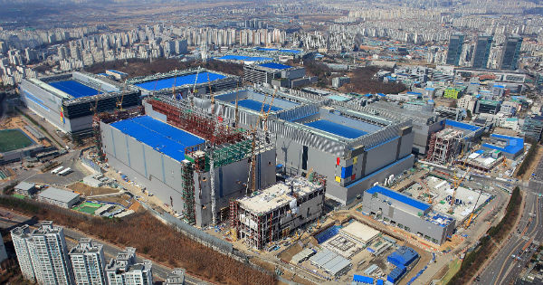
Samsung is also collaborating with customers on a customised EUV-based 6nm process node and has already received the product tape-out of its first 6nm chip. The EUV-based process technologies are currently being manufactured at the S3-line in Hwaseong, Korea. The company has also announced it will expand its EUV capacity to a new EUV line in Hwaseong, which is expected to be ramped up in the second half of 2019.
Charlie Bae, Executive Vice President of Foundry Business at Samsung Electronics, said: “In successful completion of our 5nm development, we’ve proven our capabilities in EUV-based nodes. Considering the various benefits including PPA and IP, Samsung’s EUV-based advanced nodes are expected to be in high demand for new and innovative applications such as 5G, artificial intelligence (AI), high-performance computing (HPC), and automotive. Leveraging our robust technology competitiveness including our leadership in EUV lithography, Samsung will continue to deliver the most advanced technologies and solutions to customers.“