In Eclipse MCUXpresso IDE 10.1 with integrated MCUXpresso Configuration Tools, I mentioned that I wanted to try the i.MX RT1050 processor. Well, finally my ordered board from Mouser arrived, right on time for the weekend, so I had a chance to use that ARM Cortex-M7 running at 600 MHz.

i.MX RT1050 EVK
Outline
The i.MX RT1050 is indeed an interesting device. It is an ARM Cortex-M7 running up to 600 MHz with up to 512 KByte of SRAM, but with no internal FLASH memory (‘flash-less’):

i.MX RT1050 Block Diagram (Source: NXP web site)
That device is interesting for me: image processing and number crunching demand more and more processing power and memory, and the Cortex-M4 I’m using mostly are hitting a 300 MHz ‘wall’, and the first M7 (see First steps: ARM Cortex-M7 and FreeRTOS on NXP TWR-KV58F220M) did not really bring the performance I hoped for. The solution I have explored so far was a combination of a Cortex-A core with a Cortex-M core (see Tutorial: First Steps with NXP i.MX7 and Toradex Colibri Board).
But this usually requires Embedded Linux running on the Cortex-A core: something I consider overkill or even a risk for running a real-time application. So that i.MX RT1050 really would close that gap and allow me continue to use the established Eclipse and JTAG debugging tools. NXP calls this device ‘crossover’, as it is bridging the gap between microcontroller and microprocessors.
What might be confusing is the ‘i.MX’ in that device name: It is not one of the traditional i.MX devices using an ARM Cortex-A. It has a single Cortex-M7 core, so it is more of a ‘normal’ Cortex-M like the ‘Kinetis’ or ‘LPC’ family from NXP, except that it seems to have inherited some of the complexity of the ‘real’ i.MX family. Anyway, as long I can use it with JTAG/SWD tools and get it run FreeRTOS, that should be fine.
Unboxing
I ordered my board from Mouser and it arrived after a week. The board costs around $80. It comes in a cardboard box and with a micro USB cable which is used for power and debug.
i.MX RT1050 EVK
My board is an SCH-29538 REV A3/700-29538 REV A one. On the left, above the micro-SD card socket, there are headers for an Arduino shield. The device offers two micro-USB ports and one Ethernet port. Below is a picture with the default jumper settings (click to enlarge):
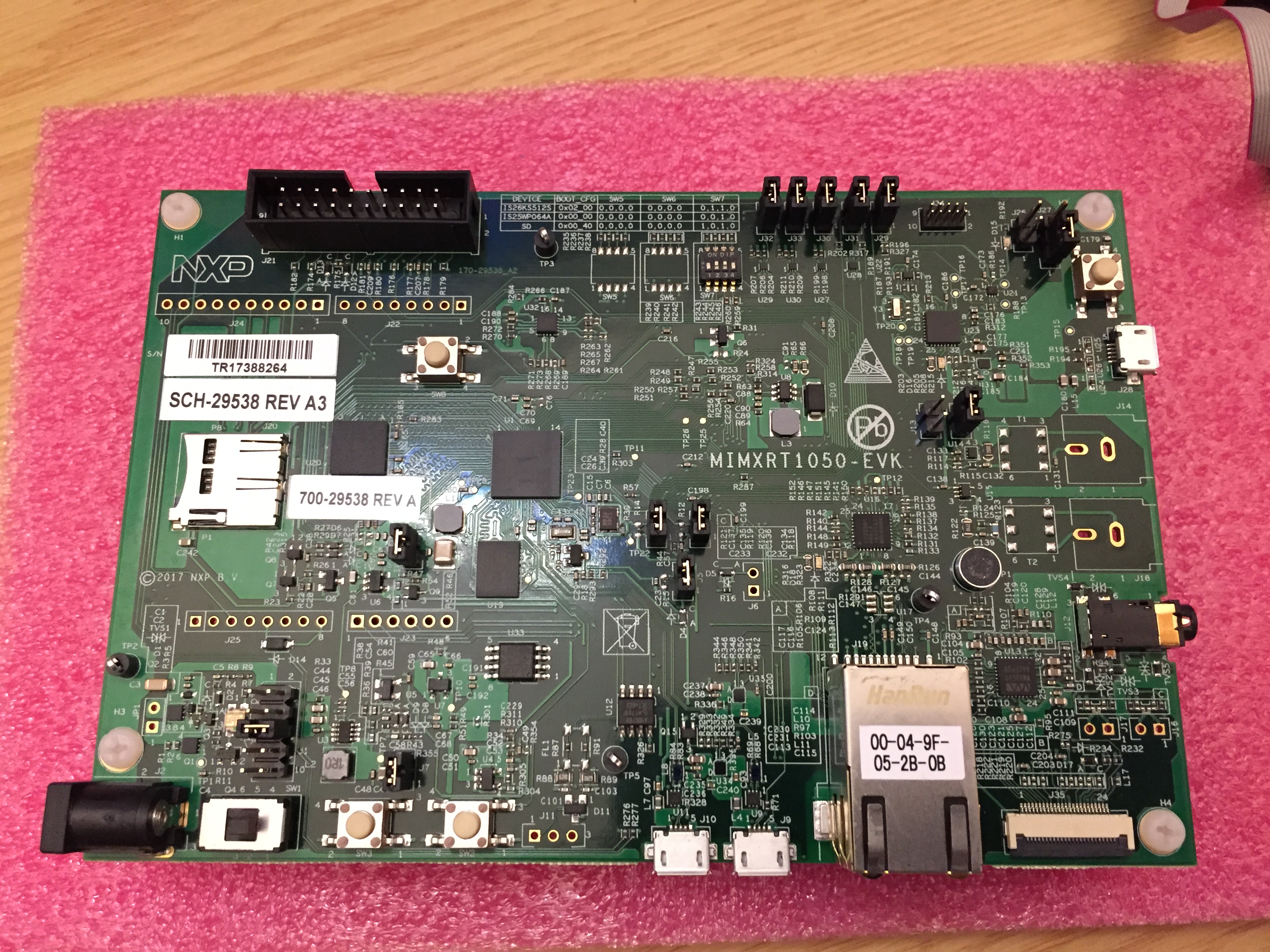
MIMXRT1050-EVK
On the backside, there are connectors for a display (left connector) and a touch interface (right connector). I guess I will try to order the matching display from Mouser too.
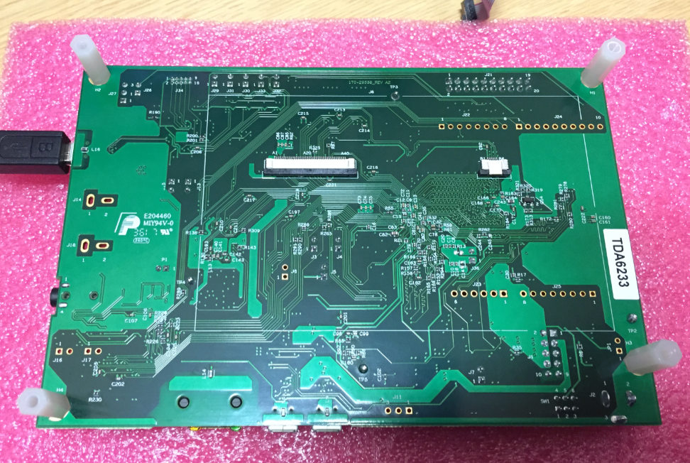
i.MX RT Board Bottom Side
The device of interest on the board is the MIMXRT1052:

i.MX RT1052 Device
Power
The board can be powered through the Debug (DAPLink/OpenSDA) USB port:

Power with DAPLink Port
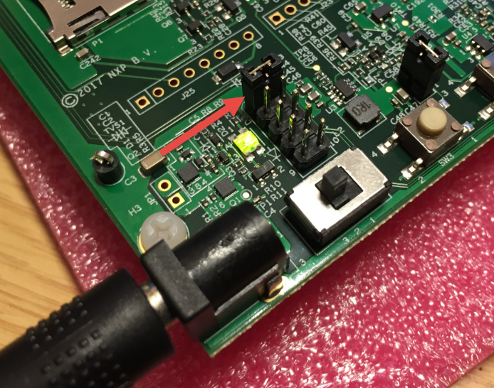
In that case, jumper J1 near the power LED should set to the *middle* position:
DAPLink Power Option
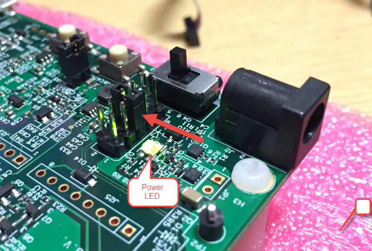
I prefer to use an external power supply, as I have faced issues with other boards if they draw too much power (and some forum posts indicate some potential USB power supply issues too). Using an external power supply, I can use the ON/OFF switch near the barrel connector. The board needs a 5V DC Power supply (Center +5V, outside GND). If using an external power source, the Jumper on J1 has to be set to the *top* position:
External Power Connector
The green LED shown in above image indicates that the board has power. More than once, I failed to debug the board because it was not powered.
Boot Options
The board can boot up from different memory using the boot option switch SW7:

SW7 Boot Options
I’m using the default option to boot from ‘Hyperflash’ with the following settings
SW7: 1-OFF 2-ON 3-ON 4-OFFMemory
In a ‘normal’ microcontroller, there is SRAM and FLASH available out of reset. As this device is ‘flash-less’ at boot time, the memory management and configuration is a bit more challenging.
The RT1052 has 512KB RAM on-chip available at boot time. It is split up into SRAM_OC (On-Chip), SRAM_ITC (Instruction-Tightly-Coupled), and SRAM_DTC (Data-Tightly-Coupled). Below, they are shown in the Memory configuration editor inside the MCUXpresso IDE:
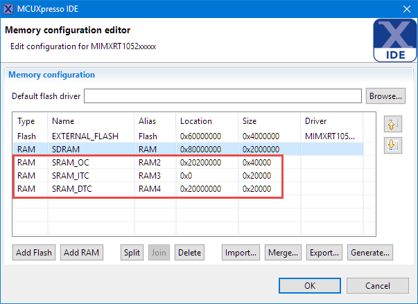
RT1052 Memory Map with on-chip RAM
The 128 KByte ‘ITC’ RAM is optimized for instruction execution, while the 128 KByte ‘DTC’ RAM is optimized for data access.
External to the RT1052 there are four extra memory options:
- 64 MByte ‘Hyper Flash’
- 32 MByte SDRAM
- 8 MByte QSPI Flash
- Micro SD card socket

RT1052 with external Memory Devices
Both the external Flash (‘Hyperflash’) and SDRAM are not available right away at boot time. The bootROM will check the external Flash for a specific header: If this header is found and valid, the Flash can be used, and it will use that information to initialize the external SDRAM too. The presence of that header is critical, as it allows executing code from that external FLASH memory, also called XIP (eXecute In Place).
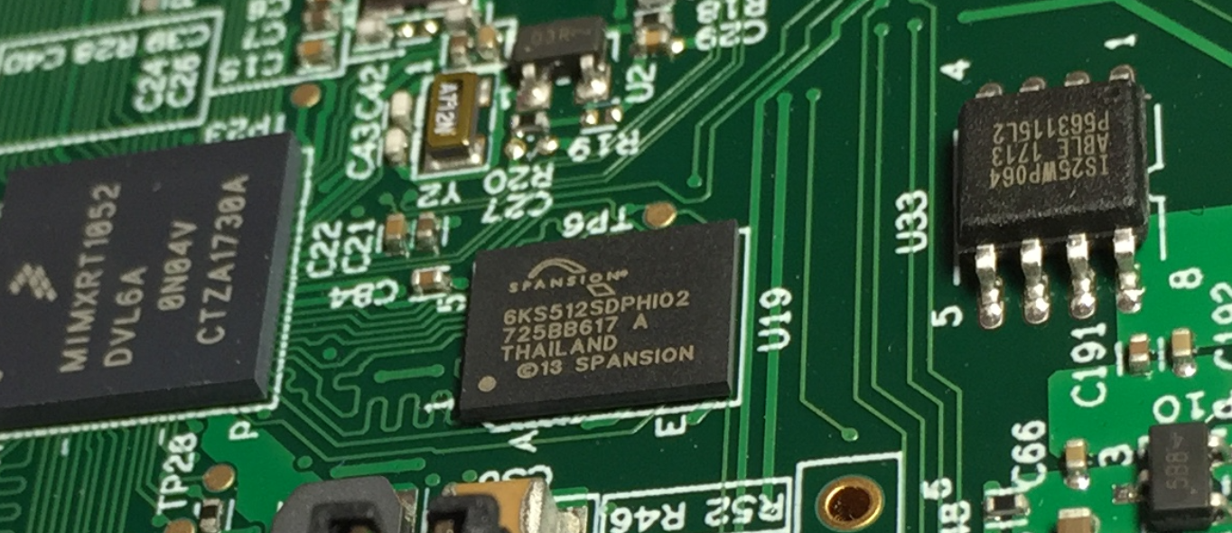
Below the 512MBit/64MByte ‘Hyper Flash’ from Spansion and the 8 MByte QSPI on the right:
Spansion Flash Device plus SPI Flash
The 32 MByte 166 MHz SDRAM device:

SDRAM
The 8 MByte QSPI Flash device:

QSPI 64MBit FLASH
It looks like the QSPI Flash is not really usable. From the user manual:
“By default, this QSPI Flash is disabled on the EVK. To enable it, Hyper Flash should be removed when the QSPI Flash is selected as the boot device. And R153, R154, R155, R156, R157, R158 should add 0 Ohm resistors.”
Does this really mean *removing* the Hyper Flash device from the board?
On-Board Debug Interface
The board's features include the DAPLink (or OpenSDA) onboard debug interface as present on many other Freescale/NXP boards.
The programmed DAPLink firmware information is:
# DAPLink Firmware - see https://mbed.com/daplink
Unique ID: 0225000041114e4500463009c207001792d1000097969900
HIC ID: 97969900
Auto Reset: 0
Automation allowed: 0
Daplink Mode: Interface
Interface Version: 0241
Bootloader Version: 0242
Git SHA: 34182e2cce4ca99073443ef29fbcfaab9e18caec
Local Mods: 1
USB Interfaces: MSD, CDC, HID
Bootloader CRC: 0x73707d49
Interface CRC: 0x92919274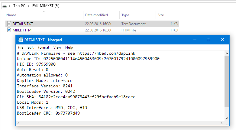
DAPLink Firmware
Because that firmware is not the latest one, I downloaded the update from http://www.nxp.com/opensda. The same link is available in the MCUXpresso IDE:

OpenSDA Firmware Update Site
There are two different firmware binaries for debugging with CMSIS-DAP: one for SPI-Flash and one for Hyper-Flash.
I have only used the Hyperflash one. I could be that the difference is where the USB MSD flashloader stores the binary. Anyway I’m not using that loader and using the debugger instead.
Because the board is initially configured to use Hyperflash, I have downloaded that firmware (I downloaded both, just in case, but make sure you use the correct one depending on your flash configuration):
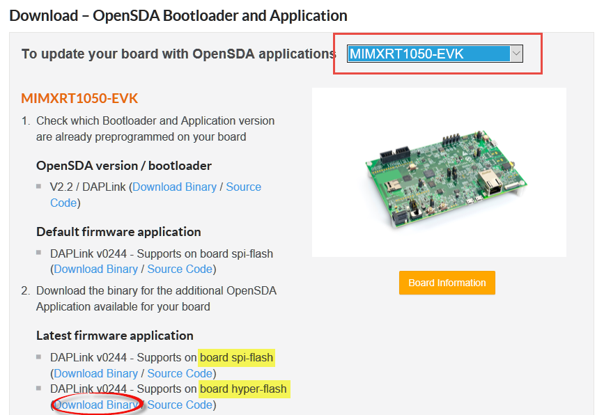
Download OpenSDA Binary
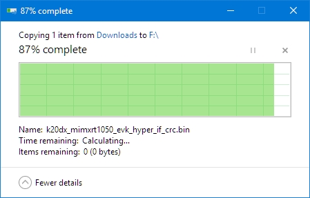
This downloads k20dx_mimxrt1050_evk_hyper_if_crc.bin for me.
To program the new CMSIS-DAP firmware:
- Power off the board
- Make sure Jumper J27 is on 1-2 position:

- Press and hold SW4 while powering the board, then release SW4
- The device should show up as ‘MAINTENANCE

- Copy the .bin firmware file downloaded to that drive/device (e.g. drag and drop)

- Power off the board and power it up again. Check the Interface Version (this is the new CMSIS-DAP Firmware version):

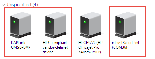
- Power off the board again. Set Jumper J27 to the position 2-3 for OpenSDA Debug
- Power on the board again. On Windows, under Devices/Printers it should show now three additional devices:

- Now we are ready to debug it.


MCUXpresso IDE
The SDK (software drivers) for the device are available from http://mcuxpresso.nxp.com/. After selecting the device I can build the SDK:

MCUXpresso SDK Page
This gives me another page of options for the SDK. Make sure to select the MCUXpresso IDE. With the ‘Add software component’ I can add extra components as FreeRTOS. Then download the SDK.

Configured the SDK
MCUXpresso IDE
I’m using the MCUXpresso IDE V10.1.0 (see Eclipse MCUXpresso IDE 10.1 with integrated MCUXpresso Configuration Tools). The downloaded SDK from the previous step gets added via drag and drop into the Installed SDK view:

Installed SDK in MCUXpresso IDE
Create a new project with the shortcut in the Quickstart Panel:
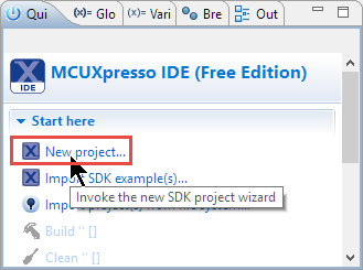
Creating New Project
Select the board, then press next:

Creating Project for 1050
In the next page, I have selected FreeRTOS (or go with the defaults):

Configure the Project
Pressing next gives the advanced options, which I keep at their defaults:
Installed SDK in MCUXpresso IDE
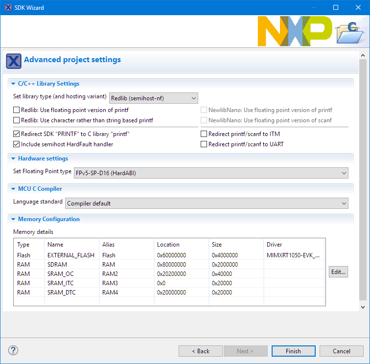
Advanced Project Options
With ‘Finish’ the project gets created, and I can build it:

Building project
Debug
My board had problems with debug, because probably the content of the external FLASH block confused the bootROM, so debugging was not possible. Consult the ‘Troubleshooting’ section at the end of this article for erasing the external FLASH first.
To debug the project, use the ‘Debug’ button from the Quickstart Panel:
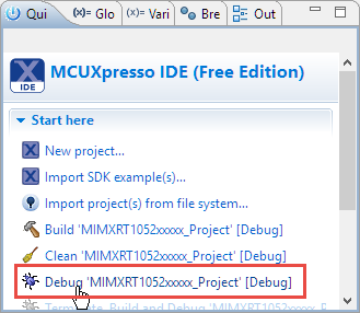
Debug from the Quickstart Panel
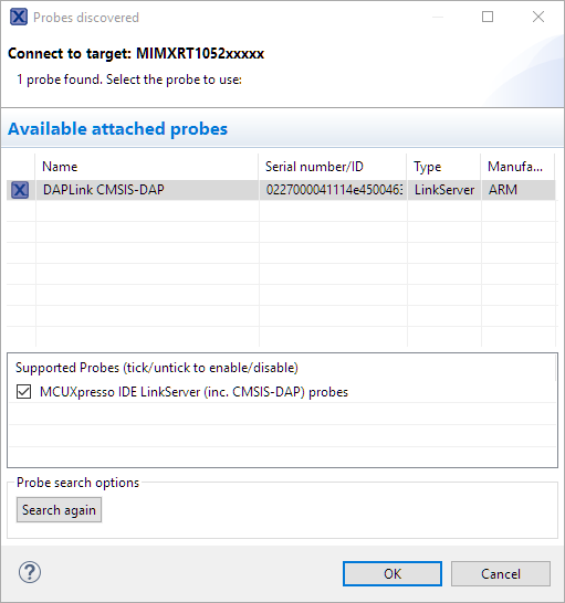
The first time, it will trigger a probe discovery, and the DAPLink probe should show up:

Probe Discovered
With this, I can debug that ‘hello world’ project in the MCUXpresso IDE:

Debugging Hello World
Execute in Place (XIP) Header
As seen from the Disassembly view above, the program is executing from the external FLASH at 0x6000’0000. The project has files in the ‘xip’ folder to create and link the needed header at address 0x6000’0000:

XIP File in Project
This creates an 8 KByte special header at the beginning of the FLASH at address 0x6000’0000:

Hyperflash Config Block
Most of the SDK examples are running in RAM. To change them to run from the external FLASH, consult the Overview Guide.
Debug Connector J21
If using an external SWD/JTAG debug probe, the board has a connector for the main CPU located on J21. In the picture below I have attached the NXP LPC-Link2 probe with a custom enclosure (see Custom 3D Printed Enclosure for NXP LPC-Link2 Debug Probes).
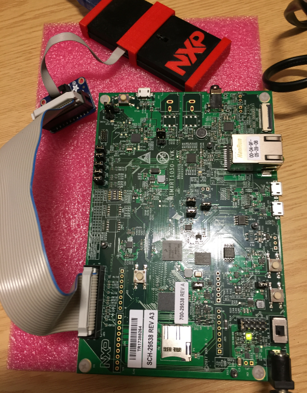
LPC-Link2 External Debug Probe
Debug connection with the P&E Multilink Universal:
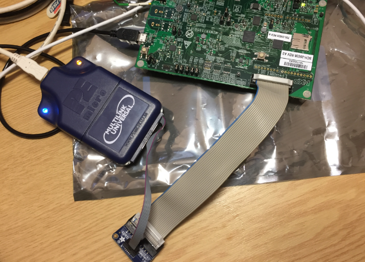
Debugging with P&E Multilink
Same with the Segger J-Link:

Debugging with J-Link
The onboard DAPLink debugger is not that fast. What helps for the LinkServer/OpenSDA debug connection is to remove the following (see Overview Guide):
--cachelib libm7_cache.so
Removing cachelib libm7_cache.so
That removes the extra cache handling, making debugging about twice as fast. Speed is ok that way, but not at par use an external debug probe. If you are really serious about debugging, get an external debug probe.
For using it with a small 2×5 0.05″ cable, I have to use an adapter board, e.g. the one from Adafruit.
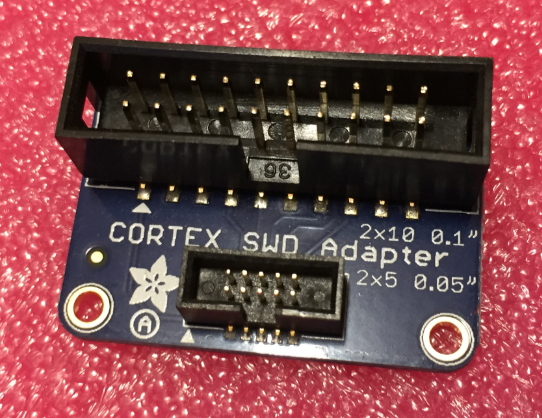
Cortex SWD Adapter
I have been able to use onboard DAPLink, Segger J-Link, P&E Multilink, and the NXP LPC-Link2 to debug the board.
Troubleshooting
I was not able to debug my board, probably because the bootROM was confused by some incorrect values in the external Hyperflash at address 0x6000’0000. To solve that problem, erase the FLASH memory. With the MCUXpresso IDE, either the onBoard DAPLink with CMSIS-DAP or the NXP LPC-Link2 Debug probe on connector J21 has to be used (the P&E or Segger probes won’t help here).
First, power off the board and change the SW7 DIP Switch to...
SW7: 1-ON 2-ON 3-ON 4-OFF...to prevent booting from Hyperflash:

Preventing booting from Flash
Power the board again. Select a project setup for XIP and start the GUI Flash Programmer in the MCUXpresso IDE:
GUI Flash Programmer Icon
The project must have a DAPLink or LPC-Link2 debug connection:
DAPLink Connection
Next, make sure that the ‘Mass erase’ option is enabled:
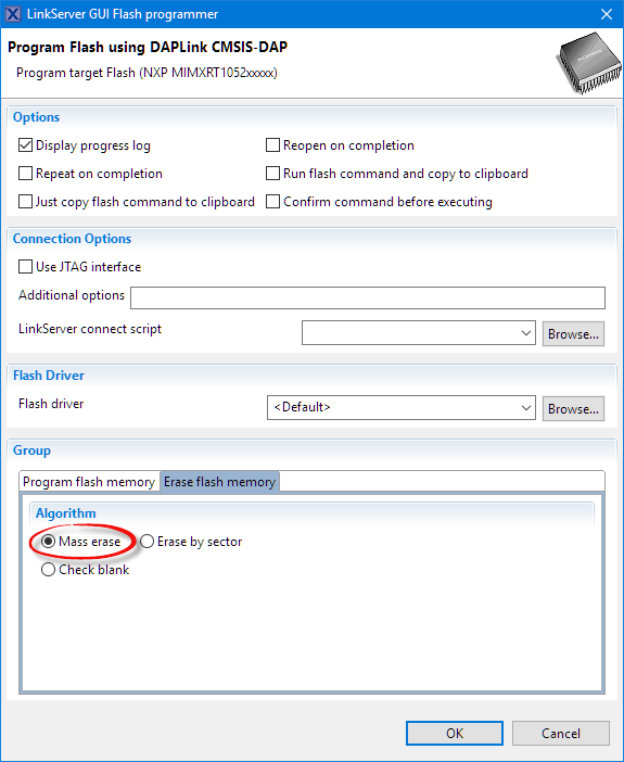
Mass Erasing Device
Press OK:

Mass Erase Progress
This will trigger the following dialog, which can be closed:
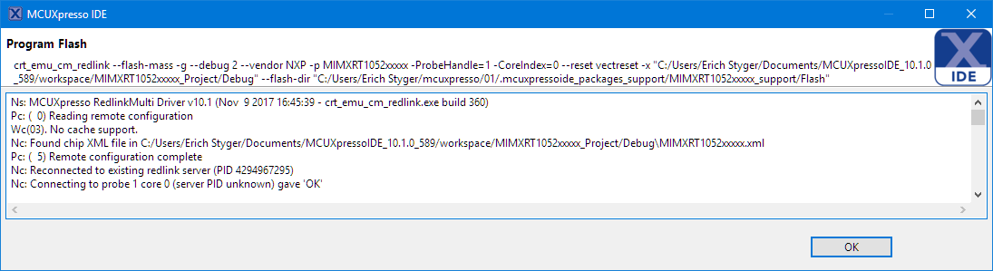
Program Flash
Power off the board, then restore the SW7 to the allow boot from Hyperflash again:

Boot from Hyperflash
Because the Hyperflash boot block is now erased, the board should be usable again.
Summary
The i.MX RT1052 is indeed an interesting device: lots of performance. According to NXP Factsheet, the price should be reasonable too: “10k resale at sub $2.50”. Still, there will be costs — at least for an external FLASH memory. That BGA package makes it tricky for hobbyists. Using the MCUXpresso IDE makes the first steps with that board a better experience. While the onboard DAPLink is convenient, I recommend using an external debug probe. Finally, maybe board vendors will come up with small and breadboard friendly breakout boards for the i.MX RT? Something like the tinyk22? That would be awesome!
Happy RT’ing!
Links
- NXP i.MX RT Web Page: https://www.nxp.com/products/processors-and-microcontrollers/applications-processors/i.mx-applications-processors/i.mx-rt-series:IMX-RT-SERIES
- Overview of using the MIMXRT1050-EVK with MCUXpresso IDE: https://community.nxp.com/community/mcuxpresso/mcuxpresso-ide/blog/2017/12/07/overview-of-using-the-mimxrt1050-evk-with-mcuxpresso-ide
- MCUXpresso IDE: http://www.nxp.com/mcuxpresso/ide
- MCUXpresso SDK: http://mcuxpresso.nxp.com/